(Click for a bigger picture)
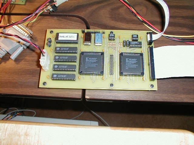
The PDP-8/X is a reimplementation of the PDP-8/I, with 32K words of memory (all the memory you can put on a PDP-8/I), an extended memory control, an interface to an RS-232 terminal, and an interface to an IDE disk, which I built just for fun.
I consider this machine to be a new model compatible with something from the past, as opposed to a clone of the past, so I feel no shame in introducing new model-specific variations. The PDP-8/X, therefore, uses IDE disks with a new disk interface, because I thought that it would not be unreasonable for a new model to come out with a new disk controller, especially considering that customer-written PDP-8 device handlers were both common and encouraged.
The following sections describe the hardware, the software, and the design methodology of the PDP-8/X in fairly broad strokes. Addition technical information is available. The reference manual contains a more detailed description of the system from a programmer's point of view. The drawings (page 1, page 2, page 3, page 4) show how everything is hooked up. Plots of the printed circuit board (top side, bottom side, both sides, silk screen) show the layout. The ROM listing file shows the details of the front panel program (it's one of those programs that just kept growing, so it isn't that pretty in spots).
Many people have asked to see the C++ programs which generate the wirelists for the two FPGA chips. The file cpu.c is the program which generates the CPU wirelist, and the file iou.c is the program which generates the IOU wirelist. The files chip.h and chip.c are the library files which do much of the work.
Here's a block diagram of the PDP-8/X system.

The CPU is implemeted by a XILINX XCS10 (SPARTAN, 5.0V, 14x14 CLBS) field programmable gate array, and contains the basic processor, the memory extension control, and a small amount of logic needed to assist with the implementation of the front panel program.
Four 32Kx8 SRAMS implement a 32Kx12 normal memory and a 32Kx12 front panel memory (of which only the lowest 4K is used). The CPU drives the address and control signals of the SRAMS.
The front panel program is stored in the low 8K bytes of a 32Kx8 EPROM, the contents of which is copied into low 4K words of the front panel memory by the CPU at reset time. The high 6 bits of each EPROM word flow directly to the high 6 bits of the SRAM. The low 6 bits of each EPROM word flow indirectly to the low 6 bits of the SRAM, passing through the CPU.
The IOU is implemented by a XILINX XCS05 (SPARTAN, 5.0V, 10x10 CLBS) field programmable gate array, and contains 2 I/O devices. The teletype device implements the standard PDP-8 terminal interface (device code 03/04). The disk device implements a simple programmed I/O interface to an IDE disk. The terminal interface also watches for framing errors, and when one is detected, a HALT REQUEST is sent to the CPU, on the assumption that the framing error was caused by the user generating a BREAK.
The CPU sends IOT instructions to the IOU over the data bus. An earlier design had the CPU sending IOT instructions to the IOU over (essentially) the memory address bus, but this made the printed circuit board layout much more tangled.
Just about any IDE disk can be used, since the PDP-8/X drives it in the slowest possible timing mode (that is, in PIO mode 0). The system currently uses a 20MB SanDisk FLASHDRIVE, so the system is silent.
Here's a block diagram of the CPU.
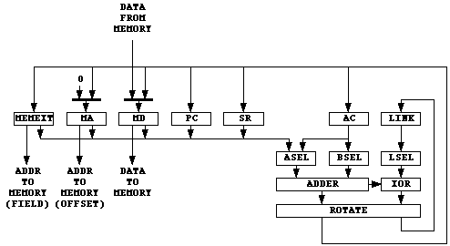
The heart of the data path is the ALU, which consists of a adder feeding a rotate box.
The adder is 12 bits wide, and uses ripple carry, which is fast enough, and has a very compact XILINX implementation. One side of the adder is fed a variety of sources, via a tri-state bus and the ASEL box. The other side of the adder is fed from the AC register via the BSEL box. The ASEL box selects between the value on the tri-state bus, 0000, the value on the tri-state bus and'ed with the AC register, and the value on the tri-state bus or'ed with the AC register; the latter two choices are a little strange, but they come for free because XILINX function generators always compute functions of 4 variables. The BSEL box selects between AC, ~AC, 0000, and 7777.
The rotate box is 13 bits wide. The adder supplies 12 of the input bits. The other input bit is fed from the LINK register, via the LSEL box (which selects between LINK, ~LINK, 0, and 1), and an XOR gate (which complements the output of the LSEL box if there is a carry out of the adder). The rotate box can rotate left or right by 1 or 2 bits.
All of the registers in the CPU, with the exception of the AC, can be driven onto the tri-state bus. All of the registers can be written from the output of the ALU. Included in the register set is the SR, a 12-bit register which contains the current value in the (soft) front panel switches.
Memory addresses are driven from the MA register (and by the IF/DF registers in the memory extension control). The page and offset bits of the MA register have separate load enables, which simplifies the implememtation of current page addressing (when only the offset part of the MA register should be updated). The MA register can also be explicitly set to 0, which is used by zero page addressing and by interrupts.
Memory data is both captured in and driven from the MD register. The original design had separate registers for read data and write data, but this made the implementation of auto-indexed indirect addressing more dificult than it needed to be.
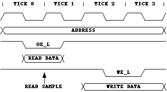
The control is based on a sequence of major cycles, each of which is a sequence of 4 ticks of the 8 MHz system clock. In general a memory or I/O read happens in ticks 0 and 1 of a major cycle, and a memory or I/O write happens in ticks 2 and 3 of a major cycle. The timing is arranged so that data read in ticks 0 and 1 can be passed through the data path and written in ticks 2 and 3, which makes things like the ISZ instruction and auto-indexing fairly straightforward. The timing of the OE_L and WE_L strobes guarantees a half-tick between read data and write data, and a half-tick of write hold.
The major cycles are similar to those of a real PDP-8. The F major cycle reads instructions. The D major cycle reads indirect addresses, and performs auto-indexing. The E major cycle executes memory reference instructions. Operate instructions, and IOT instructions which manipulate the state of the CPU itself (device 00 and device 2X), are executed in tick 2 of the F major cycle (this is possible because the soft switch register is inside the CPU; an earlier design, which stored the soft switch register in the IOU, was considered but rejected, because everything was much more complicated).
IOT instructions which manipulate I/O devices are tricky because the CPU cannot look at the instruction and determine its function. These instructions are executed by an I major state. During the read portion of the I major state the device sends a three command bits to the CPU telling it how the instruction should be executed (the command bits are an ISKP bit which says that the next instruction should be skipped, an IORA bit which says that the data being supplied during the read portion of the I major state should be combined with the AC register with an inclusive-or operation, and an ICLA bit which says that the AC register should be cleared; the sequencing is such that IORA+ICLA means load). During the write portion of the I major state the old value of the AC register (that is, before it is changed by ICLA) is made available to the device, which writes it into an internal register if it desires. The command bits are low-true and pulled up by resistors, so that if the device is unknown, the command bits are all false, which makes the IOT do nothing.
The I major cycle is unique in that it can be externally stretched to allow for slow I/O devices. Clock ticks can be added between tick 0 and 1 (stretching the read portion of the cycle) or between tick 2 and 3 (stretching the write portion of the cycle). The stretch signal is low true and pulled up by a resistor, so the default is to run at full speed.
The PDP-8/X runs a version of OS/8 V3D.
I rebuilt the system disk head from sources since it includes a new two-page system disk handler for the IDE disk. This system disk handler implements two 4095 block partitions; a SYS partition, which contains the system and the cusps, and a USR partition, which usually hold nothing precious, and which can, therefore, be zeroed with PIP should anything really bad happen.
I built the rest of the system disk by gathering bits of binary from around the web. It includes most of the cusps, and a few games, most notably CHESS and ADVENTURE. Note that ADVENTURE is written in FORTRAN, so the new two-page system disk handler is compatible with the TD8E hacks in the FORTRAN runtine.
I began development by writing a behavioural model of the system, in C++, on the Macintosh. The behavioural model implemented the CPU, main memory, the ROM, and the serial line interface, all at a very high level.
The behavioural model was used to debug the console program. Writing and debugging the console program made it clear that the first architecture for the hardware assist for the console program was far from ideal, but also suggested the design which was actually implemented. Improved designs were easy to try out because changing the behavioural model is fairly straightforward.
Once I was reasonably happy with the behavioural model, I needed to transform it into a low-level model in which every gate and register is explicitly represented. I designed the datapath around the strengths of the XILINX devices I planned to use from the start. The gates-and-registers model was also written in C++, and consisted of a single large routine, the execution of which corresponded to the execution of a single clock cycle.
The behavioural and the gates-and-registers models were subclasses of a general emulation class, so I could load a program into both models and observe differences in the execution of the program caused by differences between the two models (all of which were bugs, usually in the gates-and-registers model). I kept debugging at this stage until I could run FOCAL and most of the interesting MAINDEC programs on both models.
Next I designed the physical board. From the start I wanted to build the PDP-8/X on a two-layer printed circuit board, which strongly encouraged using through-hole components, which strongly encouraged using socketed XILINX chips in 84-pin PLCC packages. The small number of I/O pins on the 84-pin PLCC packages forced the two-chip design. I let the printed curcuit board layout define the pinout of the chips (within reason), so the schematics and the printed curcuit board layout were done at the same time. The printed circuit boards were done at EXPRESS-PCB, so I was forced to use their simple layout editor, running on a Windows PC.
With the design partitioned into two chips and the structural model done, all I needed to do was transform the logic from the model into a form which could be fed to the XILINX place-and-route software. This was not done by drawing schematics, or by describing the logic in VHDL/VERILOG and feeding it to a logic synthesis tool. Instead, I did it by describing the logic in the form of a C++ program, the output of which was a standard XILINX wirelist (in XNF format), which could be fed to the XILINX place-and-route software.
The description is very natural, looking very much like the logic equations one might expect, thanks to careful use of C++ operator overloading. For example, here is a piece of logic, extracted from the design. It implements the rotate box, which takes in a 13-bit bus called "d", and puts out a 13-bit bus called "e".
#define	RALI(i)	((i)==0 ? 12 : ((i)-1))
#define	RARI(i)	((i)==12 ? 0 : ((i)+1))

rarSel = tReg[T2] & sReg[SF] & ciOPR1 & mdReg[RAR] & ~mdReg[TWO];
rtrSel = tReg[T2] & sReg[SF] & ciOPR1 & mdReg[RAR] &  mdReg[TWO];
ralSel = tReg[T2] & sReg[SF] & ciOPR1 & mdReg[RAL] & ~mdReg[TWO];
rtlSel = tReg[T2] & sReg[SF] & ciOPR1 & mdReg[RAL] &  mdReg[TWO];
nopSel = ~ralSel & ~rtlSel & ~rarSel & ~rtrSel;
for (int i=0; i<13; ++i) {
  e1[i] = (ralSel & d[RALI(i)]) | (rtlSel & d[RALI(RALI(i))]);
  e2[i] = (rarSel & d[RARI(i)]) | (rtrSel & d[RARI(RARI(i))]);
  e[i] = e1[i] | e2[i] | (nopSel & d[i]);
}
The C++ program which generates the wirelist contains calls which attach placement and timing constraint information to the cells. I hand placed the entire datapath, partially to get a very dense placement, and partially because my C++ design package requires that all adder-like cells be placed (so it can automatically figure out how to configure the carry chains). The XILINX tools can process this wirelist very quickly because the placement tool (which is by far the slowest part of the place-and-route process) is given a small and very constrained problem.
The output of the XILINX place-and-route tools were loaded into the hardware using an XCHECKER cable attached to the parallel port of the PC. Debugging the hardware took only a couple of hours. The most powerfull debugging tool was the ability to quickly change the patterns in the XILINX chips; in particular, to change the pattern in the CPU chip so that it hung at a particular PC value, allowing the program to be "single stepped" in a way which could be observed with an oscilloscope.
At this point is was time to debug the operating system. My plan was always to bring the operating system up on the behavioural model, then verify that it worked the same way on the gates-and-registers model, and then to move over to the hardware, where, in theory, there should be no debugging at all. To this end, I embelished the behavoural and gates-and-registers models to support an emulated disk which could be loaded from and saved into disk files. The disk emulation was extremely simplistic; just enough for a disk driver which used programmed I/O.
The IDE disk interface needs a 2-page system handler. A 2-page system handler is harder to write than a 1-page system handler because there are lots of details, like the use of block 66 during bootstrapping, and the way it has to look just enough like the handler for the TD8E to fool a bunch of very tinkery code in the FORTRAN runtime system, which can only be figured out by reading a lot of code in BUILD.PA, RTL.PA, and RTS.PA. But once the tricky bits were understood, writing the handler is easy.
It's unclear to be how DEC closed the bootstrap loop with respect to BUILD and new system handlers, but here's how I did it. I read BUILD.PA and understood exactly what the LOAD command did, and then hacked up a copy of the low-speed PTR/PTP driver so that if it was loaded on top of BUILD it would appear that BUILD had loaded it normally with it's LOAD command. At this point I could proceed normally, using a LOAD command to load the system disk handler, then using the BUILD command to construct a system from OS8.BN and CD.BN, then bootstrapping the system. Only five files needed to be recompiled from source (OS8.PA, CD.PA, BUILD.PA, LSPT.PA, and AS33.PA). A few of these needed some little edits, mainly to eliminate checks for "^C on the console terminal" while loading from PTR, which is bad when the console terminal is the same device as PTR.
One I had the system running on the models, running it on the real hardware was as easy as expected. All of the grief was caused by flow control, and I got everything to work by hacking at the terminal emulator to get it to send files in 192 byte blocks (128 words, 3 bytes per 2 words) with 250 millisecond delays between them.
I actually generated a system by running BUILD on the real hardware, but as I did it I realized that there was a better way to do it. I generated the system on the behavioural model, and then downloaded the disk image (saved into a file) to the real disk. This is better because it is much easier to create a complete system image as a disk image file; you don't lose everything when you make a mistake late in the game. The block-at-a-time disk download takes a while at 9600 baud, but I didn't do it very often.
I never blasted a XILINX configuration PROM until the very end, when I was sure that the bits were as correct as I could make them. If I had used a configuration ROM which could have been reprogrammed (like the ATMEL AT17C256) I might have blasted them more often.
Updated: January 08, 2005